 | Step 1 Before you start: Ground yourself. Lightly touch your PC's metal chassis to discharge any current from your body. Then unplug the power cable. What you'll need: A phillips-head screwdriver, needlenose pliers, and antistatic wrist strap. Turn off the computer and open the case. Locate an available PCI slot for the MPEG-2 decoder card (if your kit includes one). If you're installing a SCSI drive and you don't yet have a SCSI controller in the system, you'll need a second slot for the SCSI card. |
 | Step 2 |
 | Step 3 Locate an available 5.25-inch drive bay that opens onto the front of the case. Remove the bay cover if necessary. |
 | Step 4 Configure the jumpers on your DVD drive. For an IDE drive, set the jumpers for either master, slave, or sole drive, depending on what else is on the channel. For a SCSI drive, set the jumpers to the correct ID or termination setting. |
 | Step 5 Secure the drive in the bay. |
 | Step 6 Attach the cables. Connect the DVD drive to the IDE or SCSI bus and to the power supply. Also connect the DVD drive to your sound card - or connect the decoder card (if included) to the DVD drive and sound card. (If you already have a CD-ROM drive, you can use a micro stereo patch cord to connect the external headphone jack on the DVD drive to your sound card's line-in jack). |
 | Step 7 Close the case, turn on the power, and install any necessary drivers or software. |


Thursday, January 31, 2008
INSTALLING DVD DRIVE
Sunday, January 20, 2008
ASSIGNMENT No:2-PACKAGE TYPES
Processors Package Type Guide (Desktop Processors)
FC-LGA4 Package Type
FC-LGA4 Package Type


The FC-LGA4 package is used with Pentium® 4 processors designed for the LGA775 socket. FC-LGA4 is short for Flip Chip Land Grid Array 4. FC (Flip Chip) means that the processor die is on top of the substrate on the opposite side from the LAND contacts. LGA (LAND Grid Array) refers to how the processor die is attached to the substrate. The number 4 stands for the revision number of the package. This package consists of a processor core mounted on a substrate land-carrier. An integrated Heat Spreader (IHS) is attached to the package substrate and core and serves as the mating surface for the processor component thermal solution such as a heatsink.You may also see references to processors in the 775-LAND package. This refers to the number of contacts that the new package contains that interface with the LGA775 socket. The pictures below include the LAND Slide Cover (LSC). This black cover protects the processor contacts from damage and contamination and should be retained and placed on the processor whenever it is removed from the LGA775 socket.
FC-PGA2 Package Type


FC-PGA2 packages are similar to the FC-PGA package type, except these processors also have an Integrated Heat Sink (IHS). The integrated heat sink is attached directly to the die of the processor during manufacturing. Since the IHS makes a good thermal contact with the die and it offers a larger surface area for better heat dissipation, it can significantly increase thermal conductivity. The FC-PGA2 package is used in Pentium III and Intel Celeron processor (370 pins) and the Pentium 4 processor (478 pins).
FC-PGA Package Type


The FC-PGA package is short for flip chip pin grid array, which have pins that are inserted into a socket. These chips are turned upside down so that the die or the part of the processor that makes up the computer chip is exposed on the top of the processor. By having the die exposed allows the thermal solution can be applied directly to the die, which allows for more efficient cooling of the chip. To enhance the performance of the package by decoupling the power and ground signals, FC-PGA processors have discrete capacitors and resistors on the bottom of the processor, in the capacitor placement area (center of processor). The pins on the bottom of the chip are staggered. In addition, the pins are arranged in a way that the processor can only be inserted one way into the socket. The FC-PGA package is used in Pentium® III and Intel® Celeron® processor.
S.E.C.C. Package Type


S.E.C.C. is short for Single Edge Contact Cartridge. To connect to the motherboard, the processor is inserted into a slot. Instead of having pins, it uses goldfinger contacts, which the processor uses to carry its signals back and forth. The S.E.C.C. is covered with a metal shell that covers the top of the entire cartridge assembly. The back of the cartridge is a thermal plate that acts as a heatsink. Inside the S.E.C.C., most processors have a printed circuit board called the substrate that links together the processor, the L2 cache and the bus termination circuits. The S.E.C.C. package was used in the Intel Pentium II processors, which have 242 contacts and the Pentium® II Xeon™ and Pentium III Xeon processors, which have 330 contacts.
CPGA (Ceramic Pin Grid Array)

CPGA stands for Ceramic Pin Grid Array, a type of connection for CPUs where the processor's die is attached to a heat-conducting ceramic plate which is pierced by an array of pins which make the requisite connections to the socket.
Popular CPUs that employ CPGA are the "classic" Socket A Athlon and the Duron, both from AMD.
OPGA (Organic Pin Grid Array )

The Organic Pin Grid Array (OPGA) is a type of connection for integrated circuits, and especially CPUs, where the silicon die is attached to a plate out of an organic plastic which is pierced by an array of pins which make the requisite connections to the socket.
CPU SOCKETS
Socket 370 (PGA370)
Socket 370 (also called PGA370) is a PGA socket designed to work with Intel Celeron and Pentium III processors in Pin Grid Array (PGA) package. There are three different revisions of the socket 370:
- Originally the Socket 370 (PGA370) was designed for Celeron Mendocino CPUs. These processors were manufactured in plastic PGA (PPGA) package, ran at speeds 300 MHz - 533 MHz, and had 66 MHz front-side bus and 2V core voltage. Original Socket 370 is not compatible with Coppermine and Tualatin Intel processors. It is possible to run Coppermine processors in this socket with the help of special PPGA-to-FC-PGA adapters, for example, PowerLeap PL-NeoS370.
- To support newer Coppermine Celeron and Pentium III processors Intel revised specifications for the socket 370. The revised socket was mechanically compatible with the original specification, but there were differences in electrical specifications. As a result, new Coppermine CPUs would not work in the original socket, even though they would fit into it. Revised Socket 370 supported Coppermine processors running at speeds 533 MHz - 1133 MHz with FSB 100 and 133 MHz and core voltages in the range from 1.5V to 1.8V. Tualatin Pentium III processors were not directly supported by the socket, though it was possible to run them in the socket with the help of Tualatin adapters (for example, PowerLeap Neo/T). Many motherboards with this PGA370 socket revision also supported Celeron processors in PPGA package.
- With the introduction of new Tualatin Pentium III core the socket 370 was revised once again. Like the previous revision of the socket, the second revision was mechanically compatible with old sockets, but electrically incompatible with previous socket revisions. This socket revision supported Tualatin processors in the range from 1 GHz to 1.4 GHz with FSB 100 and 133 MHz and core voltages 1.45V and 1.5V. Majority of motherboards with this revision of the socket 370 were also compatible with older Coppermine Pentium III and Celeron processors.
Visually it's not possible to distinguish between different revisions of the socket 370 (PGA370), they all look like the socket on the picture below:

The socket has 370 pin-holes - hence the name Socket 370, and it has the same size as the Socket 7. There are two differences between these sockets:
- Socket 370 processors don't have 2 corner pins while Socket 7 processors don't have only one corner pin. The extra corner pin doesn't allow Socket 7 processors to fit into PGA370 socket.
- There are 6 rows of pins between the edge and the center of the processor for Socket 370 processors, and 5 rows for Socket 7 processors.

Socket 462 (Socket A) | ||
|---|---|---|
Socket 462 (also called Socket A) is a PGA socket designed for AMD K7 family of processors. This socket can be used with AMD Athlon and Duron processors ranging in speed from 600 MHz to 2200 MHz (3200+) and with bus frequences ranging from 100 MHz to 200 MHz (400 MHz DDR). For a full list of supported processors please see below.
Socket A has 462 pin holes (hence the name "Socket 462") with 11 pluged pin holes. Socket dimensions are 5.59 cm (5.24 cm without lever) x 6.55 cm or 2.2" (2.06" without lever) x 2.58", which is almost the same as Socket 7/Super Socket 7. Supported processorsAthlon (Socket A) (600 MHz - 1400 MHz) Athlon 64, 64 FX, Sempron 64 and Opteron processors use different type of socket. There are no Intel or VIA processors compatible with this socket. NOTE: Not all processors may be supported by all motherboards. Please see "Upgrading socket 462 motherboards" section below on how to determine what microprocessors can be supported by your motherboard. Compatible socketsNone. Compatible package types462-pin ceramic Pin Grid Array (PGA) package, 462-pin organic PGA. Upgrading socket 462 motherboardsWhile you can fit many socket 462 processors into your motherboard, not all of them may be supported by the board. To determine what processors are supported you'll need to:
To determine upgrade options for brand name computers (like Dell or HP) try to search for computer model on computer manufacturer website. For upgrade information for ASUS, DFI, ECS, Gigabyte Technology, Jetway, MSI and PC Chips motherboards please check CPU-Upgrade motherboard database. |

Thursday, January 17, 2008
MOTHERBOARD FORM FACTORS
AT (form factor)
The AT form factor was the first modern motherboard form factor to be widely used. AT (Advanced Technology) was released in 1984 by IBM. Unlike the PC and XT form factors that preceded it, AT became a widely used design during the booming home computer market in the 1980s. IBM clones made at the time began using AT compatible designs, contributing to its popularity. In the 1990s many computers still used AT and its variants. Since 1997, the AT form factor was largely supplant by ATX.
Design 
 Baby AT motherboard.
ATX form factorDesign
The original AT motherboard, later known as "Full AT", is 12 inches (305 mm) wide and 13.8 inches (350 mm) deep, which means it will not fit in "mini desktop" or "minitower cases". The board's size also means that it takes up space behind the drive bays, making installation of new drives more difficult. The power connectors for AT motherboards are two nearly identical 6-pin cables. Unfortunately, the two power connectors it requires are not easily distinguishable, leading many people to damage their boards when they were improperly connected. When plugged in, the two black wires on each connector must be adjacent to each other, creating a row of 4 black wires (out of the total 12) and a correct connection. Technicians developed mnemonic devices to help assure proper installation, including "black wires together in the middle" and "red and red and you are dead."
Variants

In 1985 IBM introduced Baby AT. Soon after all computer makers abandoned AT for the cheaper and smaller Baby AT, using it for computers from the 286 processors to the first Pentiums. These motherboards have similar mounting hole positions and the same eight card slot locations as those with the AT form factor, but are 2" (51 mm) narrower and marginally shorter. The size (220x330 mm) and flexibility of this kind of motherboard were the key to success of this format. While now obsolete, a few computers are still using it, and modern PC cases are generally backwards compatible to fit Baby AT.
In 1995, Intel introduced ATX, a modern form factor which gradually replaced older Baby AT motherboards. During the late 1990s, a great majority of boards were either Baby AT or ATX. Many motherboard manufacturers continued making Baby AT over ATX since many computer cases and power supplies in the industry were still compatible with AT boards and not ATX boards. Also, the lack of an eighth slot on ATX motherboards kept it from being used in some servers. After the industry adapted to ATX specifications, it became common to design cases and power supplies to support both Baby AT and ATX motherboards.
The ATX form factor is a replacement for the older AT and baby AT form factors. Invented by Intel in 1995, it incorporates the first major change in the layout of PC motherboards to occur in years. The ATX motherboard rotates the orientation of the board 90 degrees. This allows for a more efficient design, with disk drive cable connectors closer to the drive bays and the CPU closer to the power supply and cooling fan. All Intel motherboards currently produced are ATX motherboards. Generally speaking, an ATX motherboard is required to use the newest Intel processors. Because of this and the general improvements that ATX brings, the ATX form factor is the form factor of choice for both commercial mass-production systems and for home PC builders.
ATX motherboard and case design
The ATX case looks very similar to the baby AT case, except that the holes in back for ports and keyboard and mouse connectors have been altered to allow for the different design of the ATX motherboard. In particular, the ATX motherboard has integrated I/O ports mounted directly on the edge of the board. Most ATX motherboards have, from left to right, stacked keyboard and mouse ports, stacked USB ports, printer and game ports along the top, and two serial ports along the bottom. This design can differ based on the manufacturer of the motherboard. This allows for a much more effective use of interior case space, and decreases the number of cables and connectors that can become disconnected or damaged.
ATX cases often have more drive bays for a given case size. For example, a mid-tower ATX case will often have more available drive bays than a baby AT case of the same size. The ATX case design also generally provides easier interior access to expansion bays.
The ATX power supply is different in a number of important ways. ATX power supplies and motherboards function at 3.3 volts or lower, instead of 5 volts, reducing motherboard cost, energy consumption, and heat production. The fan on the power supply is reversed so that it blows air into rather than out of the case, which helps keep the case clean and reduces heat buildup. This is necessary due to the high heat produced by the new generation of Intel Pentium II/III and AMD processors. The ATX power supply is turned on and off using electronic signaling instead of a physical toggle switch. This allows the computer to be turned on and off using software control, thus improving power management and energy-saving features. Because of this, ATX power supplies must be matched with ATX motherboards.
BTX(Form Factor)
BTX (Balanced Technology eXtended) is a new personal computer form-factor that has been designed to replace the ATX case and motherboard layouts our computer components are currently built around. At the moment it is an Intel-only proposed standard, as AMD currently has no plans to support the BTX form-factor. There is no reason why it couldn't in the future though The form-factor of a computer affects the case layout, the positioning of components on the motherboard and the power supply positioning and connections. It allows motherboard, case and power supply manufacturers to know that their products will inter-operate with other parts designed to the same standard. BTX, proposed by Intel and recently ratified, makes some fairly radical changes to case and motherboard design in order to provide increased cooling for the components that need it most: the processor, chipset and video card. To put it simply, these components are moved so that they can all be effectively cooled by the airflow passing through the case. The case itself is modified so that front and rear vents are available to send the required airflow across the motherboard and out the rear of the computer. The rest of the motherboard components have also been shifted to accommodate all this positioning. Effectively, the BTX form-factor attempts to standardize case cooling so it can provide a steady flow of fresh air that modern components desperately need, while minimizing the amount of noise necessary to deliver it. The motherboard redesign will allow this to happen with a minimum of active cooling, with a single 'thermal module' both cooling the processor and creating the stream of air that will cool the other components. BTX Changes: Thermal Solutions and Motherboard The most obvious change to the motherboard is how the heatsink interfaces with it. The orientation of the processor heatsink has been altered from the standard downward facing fan/heatsink design to one that blows air through from side-to-side. Instead of the comforting, fan-topped hunk of aluminum or copper we've all become familiar with, BTX introduces something completely new, the 'thermal module.' The so called thermal module consists of the heatsink, fan, and fan duct. Dell, to name just one manufacturer, has long been using air ducts to reduce noise from inside the PC, while at the same time cooling its PC's internal components just as effectively. The thermal module takes this one step further. Combining a single large fan, a heatsink for the processor and some form of ducting to guide airflow, the thermal module will be the key for effective cooling of BTX systems. 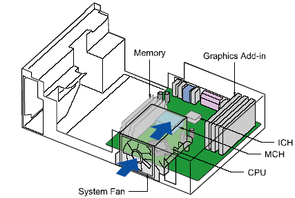 For example, ATX cases can be designed to accommodate ATX motherboards, since according to the standard, the case manufacturers know exactly where the I/O ports are going to be, and where the PCI expansion ports need to be placed. Likewise, ATX motherboard manufacturers know how many screw holes to place in their boards and where they need to be positioned to fit ATX cases, etc.
 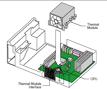 Let's run through the actual changes that the BTX standard makes to traditional ATX components, as there are a few other developments to consider.
COM Express is the PICMG industry standard for Computer-on-Modules, developed with embedded industry participation under the sponsorship of Intel, Kontron, PFU, and RadiSys.
The goals of the COM Express standards effort include the creation of specifications for small-form-factor modules to satisfy all performance segments of the embedded industry. For example, high-performance segments can use COM Express to replace PCI-X and AGP with PCI Express and replace parallel ATA with Serial ATA. COM Express also provides a bridge between legacy-free and legacy functions by incorporating optional PCI and IDE interfaces.
According to Wade Clowes, vice president and general manager of RadiSys Commercial Segment, "COM Express makes it an order of magnitude easier to configure a range of embedded products. RadiSys customers will be able to offer a line of products from low-end to high-end, using the same carrier board and swapping-out the COM module."
Functional Overview
COM Express is designed as a CPU-agnostic standard that will enable the embedded industry to adopt all-LVDS interfaces, while maintaining support for legacy interfaces, as illustrated in Figure 1.

Figure 1
COM Express board-to-board connectors consist of two rows of 220 pins each. Row AB, which is required, provides pins for PCI Express, Serial ATA, LVDS LCD channel, LPC bus, system and power management, VGA and TV-out, LAN, and power and ground interfaces. Row CD, which is optional, provides SDVO and legacy PCI and IDE signals next to additional PCI Express, LAN and power and ground signals.
COM Express provides support for:
- Up to 32 PCI Express lanes with 80-gigabit per second (Gbps) aggregate bandwidth
- External x16 PCI Express graphics
- Up to four Serial ATA-150 links with 600-megabyte per second (MBps) aggregate bandwidth
- Up to three 1-Gbps Ethernet ports, with provision for 10-Gbit Ethernet in the future
- Up to eight USB 2.0 ports
- Up to two channels of LVDS
- Up to two channels of Serial DVO
As shown in Figure 2, COM Express includes two module footprints, a compact Basic Form Factor measuring 125 mm x 95 mm and an Extended Form factor of 155 mm x 110 mm. These form factors share the same connector and signaling definitions and have overlapping mechanical assemblies. This makes it possible to interchange a Basic Form Factor module with an Extended Form Factor module, and vice versa. The Extended Form factor makes room for double the memory capacity and dual-channel memory configurations, in addition to larger processors and chipsets. Standardized height and heat spreaders further facilitate interchangeability between modules from different manufacturers.

Figure 2 COM Express footprint definitions, including Basic Form Factor (top) and Extended Form Factor (bottom)
The Extended Form Factor has a power budget of 160 Watts to support larger processors and chipsets. It also can accommodate dual-channel memory configurations. Standard height and heat spreaders facilitate interchangeability.
The form factor flexibility of COM Express enables developers to segment their designs for different classes of embedded applications, noted Kishan Jainandunsing, vice president of Technology and Business Development at PFU Systems. "The Basic Form Factor is extremely well suited for highly power sensitive, small devices such as portable applications for medical imaging and test and measurement. The Extended Form Factor is a good choice for mobile or stationary applications where performance is more important than low power dissipation, such as 4D ultrasound machines, arcade gaming devices, multimedia kiosks and electronic advertising billboards. Interchangeability between the two form factors is a bonus."
LPX Form Factor
One power supply form factor that has given Baby AT a run for its money over the last 15 years has been the LPX form factor. The "LP" in "LPX" stands for "low profile", another name given to these power supplies. They are also often called "slimline" power supplies because LPX cases are often called slimline cases, and "PS/2" power supplies after the famous IBM model. The main goal of this form factor is size reduction. The height in particular of the power supply is significantly reduced, facilitating the design of much smaller, consumer-oriented PCs. The connectors of the LPX form factor power supply are the same as that of the Baby AT and AT.
|
Diagram of the side and rear views of an LPX form factor power supply, |
Original image © PC Power & Cooling, Inc. |

While never officially specified as a standard, the LPX or "slimline" power supply basically became one anyway. Due to its small size and convenient rectangular shape, these power supplies were put into all sorts of cases; not just LPX cases but Baby AT and even full-sized AT cases. Until the rise of its anointed successor, NLX, LPX systems were made in large quantity, and millions of these power supplies are still in use.
|
Rear view of an LPX power supply, showing its power |

MINI ITX
NANO-ITX
 Via Technologies has revealed the latest member of its diminutive nano-ITX form-factor motherboard family. The Epia NR combines a fanless 1.0GHz Via C7 processor with a high-integration CX700 core-logic chip, targeting healthcare, industrial automation and digital signage, the company said.

(Click to enlarge)
The Epia NR is related to nano-ITX boards Via introduced in March, but, in what the company claims is a first, natively supports LVDS in two single- or one dual-channel monitor configuration without the need for a daughterboard. Via's Epia LT, a mini-ITX board with similar capabilities, was announced in June.
Thanks to the low-power C7 processor, among other power-stingy components, the board can operate at claimed typical power consumptions below 15.5 watts. Additionally, Via's Padlock Security Engine technology offers "military grade encryption and superior data security," the company said.

(Click to enlarge)
Key features of the Epia NR, as listed by Via, include:

(Click to enlarge)
Via says the Epia NR nano-ITX motherboard is compatible with "all leading embedded and desktop operating systems," including Windows XP Embedded, Windows XP/2000, Windows CE, and Linux.
Availability
Pre-production samples of the Epia NR motherboard are immediately available for project (volume) customers, with limited production quantities expected in early August, the company said. Pricing was not disclosed.
VIA Mini-ITX Mainboard Form Factor: 17cm x 17cmThe Mini-ITX mainboard form factor is a highly integrated native x86 mainboard measuring only 170mm x 170mm and enables the development of an infinite variety of small form factor PC systems. More than 33% smaller than the FlexATX mainboard form factor, the Mini-ITX is aimed at the development of Thin-Clients, wireless network devices, digital media systems, set-top boxes and more.
A key advantage of the Mini-ITX mainboard is that it is based on the low power VIA processor platform that comprises of either a VIA C3™ processor or a fanless VIA Eden™ ESP processor, together with a choice of highly integrated VIA chipsets and VIA companion chips.
|
VIA EPIA Mini-ITX Mainboard from VIA Embedded Platform DivisionThrough its mainboard business unit VIA Embedded, VIA produce the VIA EPIA Mini-ITX Mainboard for small, quiet PCs ranging from silent desktops to digital media rich Hi-Fi and entertainment PCs. You can download high and low resolution pictures, BIOS, drivers, manuals, and datasheets for VIA EPIA Mini-ITX mainboards from the VIA Embedded website. Trailblazing into an exciting new market, there is an increasing number of independent chassis, power supplies and other accessories manufacturers for the Mini-ITX form factor. For information on where to buy VIA Embedded Mini-ITX mainboard as well as information on what chassies are available, please go to the VIA Arena web site or contact our VIA Embedded channel partners from the VIA Embedded web site. |
VIA EPIA Mini-ITX Case Mods and Car PC ProjectsWith the I/O ports as the tallest components on the board (including the CPU cooler), the Mini-ITX mainboard is also becoming increasingly popular among the rapidly emerging enthusiast user group. The small size, quiet operation and low profile of the VIA EPIA Mini-ITX makes it ideal for moving the PC to different parts of the home, from stylish case modifications for the living room to in-car PCs. With the VIA EPIA Mini-Itx, your imagination is its only limitation! |
 The Mini-ITX mainboard successfully integrates various combinations of readily-available chipset and processor components from VIA that come with rich feature sets that include ultra low power native x86 processors, onboard LAN and various integrated AGP graphics and audio options. Further enhancing its versatility, the Mini-ITX mainboard can include CompactFlash and CardBus slots, TV-Out connector, SPDIF 5.1 audio, USB 2.0, 1394 (Firewire), integrated MPEG2/MPEG4 decoding, support for up to DDR400, Serial ATA and much more.
  VIA processor platforms are unique in that the workload is shared across the whole platform rather than being focused on the CPU, i.e. platform centric as apposed to CPU centric. Due to their low power consumption, these platforms generate less heat and therefore require less active cooling, allowing the use of quieter, lower profile coolers that are better suited to the ergonomic, small form factor systems that have more application flexibility than the more traditional tower PC.
NANO-ITX
Via Technologies has revealed the latest member of its diminutive nano-ITX form-factor motherboard family. The Epia NR combines a fanless 1.0GHz Via C7 processor with a high-integration CX700 core-logic chip, targeting healthcare, industrial automation and digital signage, the company said.
(Click to enlarge)
Thanks to the low-power C7 processor, among other power-stingy components, the board can operate at claimed typical power consumptions below 15.5 watts. Additionally, Via's Padlock Security Engine technology offers "military grade encryption and superior data security," the company said.

(Click to enlarge)
Key features of the Epia NR, as listed by Via, include:
- Processor -- Via C7 processor in NanoBGA2 package, clocked at 1.0GHz
- Chipset -- Via CX700 Unified Digital Media IGP Chipset
- Memory -- SODIMM socket, for up to 1GB DDR2 533 DRAM
- Storage interfaces:
- UltraDMA 133/100
- 2 serial ATA
- UltraDMA 133/100
- Graphics:
- integrated VIA UniChrome Pro II 3D/2D AGP graphics with MPEG-2 video decoding accelerator
- LVDS panel pin connector for 2 single-channel LVDS panels or 1 dual channel panel (optional)
- VGA port
- integrated VIA UniChrome Pro II 3D/2D AGP graphics with MPEG-2 video decoding accelerator
- LAN -- choice of Via VT6107 10/100Mbps Fast Ethernet controller, or Via VT6122 Gigabit Ethernet controller (manufacturing option)
- Audio:
- Via VT1708A high definition audio codec
- line-in/out, mic-in, S/PDIF out
- Via VT1708A high definition audio codec
- Other I/O ports:
- 6 USB 2.0 ports
- LPC bus
- SMBus
- 2 serial ports (COM1 5V/12V selectable)
- Type I CompactFlash slot (shared with IDE, default slave)
- PS2 keyboard/mouse
- 6 USB 2.0 ports
- Expansion -- 1 Mini-PCI Slot
- Size -- 4.7 x 4.7 inches (120 x 120 mm)

(Click to enlarge)
Via says the Epia NR nano-ITX motherboard is compatible with "all leading embedded and desktop operating systems," including Windows XP Embedded, Windows XP/2000, Windows CE, and Linux.
Availability
Pre-production samples of the Epia NR motherboard are immediately available for project (volume) customers, with limited production quantities expected in early August, the company said. Pricing was not disclosed.
Subscribe to:
Posts (Atom)

.jpg)
